
EE|Times/ — Mixx Technologies, Inc.
The link budget is the industry’s measuring tool as the transition to scale-up optics heats up. The largest recoverable losses are found at the connector and inside the silicon photonics platform.
Every optical networking platform today has been defined by link budgets, which account for every power gain or loss within a network, determining whether a signal is strong enough to reach the receiver and function properly. That remains the right lens for the materials now contesting scale-up optics. Silicon photonics, vertical-cavity surface-emitting lasers (VCSELs), thin-film lithium niobate (TFLN), micro-LEDs, and indium phosphide are all under evaluation. Demonstrations can show whether a material can carry the signal. Still, the link budget remains the measuring stick that will determine if they can carry the signal at the power, density, and cost a deployment requires. In scale-up optics, every recovered dB becomes architectural headroom, and ultimately, economic advantage.
Indium Phosphide has made a strong showing. High-density applications demanded by scale-up architectures challenge it. TFLN is making real inroads, historically supplying the reference modulators used for equipment and validation work. It is now pivoting into pluggable transceivers, and remains largely a pluggable transceiver platform today. That is a different adoption path, making its timing for scale-up different, not weak. VCSELs and micro-LEDs are both under evaluation as promising paths that still need to be proven.
Silicon photonics stands out as a solution for high-density scale-up. Despite the knocks against it being high power and limited reach, we need to be clear: those criticisms are not a reason to look elsewhere. They are an engineering problem that has to be solved. The useful question is not which exotic material achieves the most favor, but rather which architecture can close the end-to-end link budget at the density the system requires. Exploring where the laser power actually goes, and why the largest losses accumulate where they do, we’ll find that the answer runs through the least glamorous piece of hardware in the system (and why that’s the point).
The performance of these materials matters, but it is only one aspect in a larger system. The source, connector, optical engine, platform, receive path, and electrical recovery all draw from the same power. You can’t separate a material choice from the architecture and process decisions around it. This is why link budgets define every platform that makes it to production.
For silicon photonics, the link budget is the hardest problem that we have, and it only seems to get harder with co-packaged optics emerging. The laser is disaggregated. Because it can’t be integrated on the same package, the architecture adds a link that the laser must overcome. Higher modulation bandwidths add loss inside the silicon photonics platform, but laser power is not scaling at the same rate. The engineering challenge is real. For silicon photonics, the case for scale-up rests on whether the complete path can be made lower loss and validated as an integrated link. The link budget is the defining design factor.
Higher laser power means higher platform loss, which in turn degrades optical signal integrity. This degradation becomes electrical noise, which forces forward error correction (FEC). These power margins stacked into the link budget are what FEC exists to correct.
In a June article, Geoff Tate framed the scale-up transition as a contest decided by two link budgets: the dB link budget and the dollar link budget. In his analysis, he found that on the order of 99% of laser power is lost before hitting the receiver. This clearly demonstrates the design issue in clear terms. You cannot treat optical loss and cost as two separate problems, because the power consumed before detection becomes part of both. The path from decibels to dollars is remarkably short.

WHERE THE POWER GOES
Start at the source and follow the power from the laser to the photodiode. A 100 mW laser is roughly 20dBm at the start of the signal chain. That figure is the entire budget, and is not what the receiver registers. The laser produces a fixed amount of optical power, and every station in the path extracts a cut of it before the photodiode is paid.
The loss of power starts at the laser source itself, and accumulates at the connector that enters the optical engine. More loss is achieved as the signal crosses the silicon photonics platform, where modulation and the internal optical path consume their share of the power margin. Once it advances to the receiver side, the connector path becomes another station for power loss before the photodiode can convert what is remaining of the optical signal. By that time, most of what the laser has produced was spent along the way.
The connector path and the platform together consume the large majority of the available link budget. The specific split between them is about 60/40. This is where engineering effort can find the most recoverable margin. Before examining this, it must be understood that a higher-output laser does not, by itself, solve the architectural problem. The signal has to survive the platform and reach the detector with adequate integrity, while avoiding transferring excessive FEC work into the electrical domain. The source, optical path, and electrical recovery remain coupled.
The bottom line: The connector and the platform are where recoverable margin can be found. Reduce loss there, and the system can decide how to leverage the recovered budget. Leave the loss in place, and the system will pay for it elsewhere in the signal chain.
THE CONNECTOR
The first question you might ask is why the connector loss is so high? The simple answer is that no one owns the path end-to-end. The connector ecosystem is distributed across the fiber maker, the connector assembly company, the connector company, and the silicon photonics provider. The link budget is not set by any single point; it accumulates across the seams between four separate ecosystems.
Consider what the connector has to do. There are three points of energy loss within it, including the waveguide-to-lens interface, the lens-to-fiber interface, and the waveguide interface itself. This first interface includes the mode-expansion taper, which is the hardest piece of this challenge. It has to expand the optical mode 30x at the lowest possible loss, and then consistently maintain it. It is a triangular structure that is almost like how light expands in a torchlight, with the mode opening gradually as it moves through the taper. The taper design is tightly tied to the process that forms it, meaning it’s not a part you buy, but a structure that you fabricate.
Getting to 30x is itself hard; the industry today is still working toward a three- to five-micron mode, an expansion on the order of 10x. Maintaining this is the bigger challenge. The silicon photonics process has to expand the mode consistently, and every interface after it has to hold it through different material systems, each with its own manufacturing tolerances, until the light reaches the fiber. It’s a multi-physics problem spanning thermal, mechanical, and optical combined.
Now consider who builds the path. The fiber, connector assembly, connector, and silicon photonics interface arrive from separate ecosystems. The loss between these separate parts becomes a shared link budget when the path is fully assembled. Each provider engineers to its own specifications, each taking its share of the budget. None of this is bad work by any one company; the loss is structural. It’s easy to see why loss figures for the connector end up being around 2.5 to 3 dB of coupling loss.
Given these factors, it becomes clear why the connector is the lever. It sits at the point where process design, optical mode control, assembly, and system margin all meet. By bringing these pieces together in a common design framework, it creates an opportunity to reclaim a significant portion of the link budget.
THREE LINK BUDGET RECOVERY VECTORS
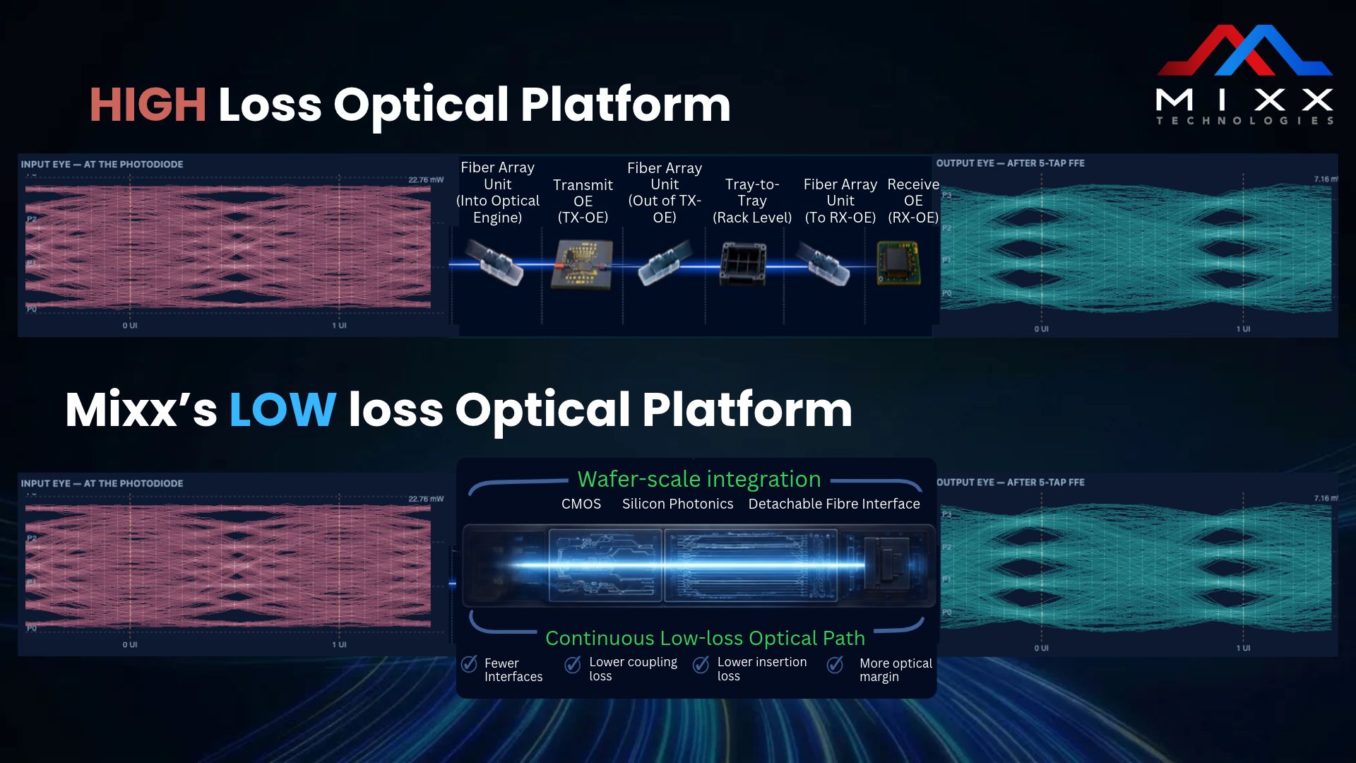
We are bringing the whole path under one roof through Mixx’s HBxIO platform, delivering an end-to-end optical signal chain into a unified design and process boundary. In doing so, we’ve been able to engineer the recovery of the link budget along three vectors.
The first vector is the connector, where Mixx’s SxC™ is a top-down integrated connector achieving an end-to-end waveguide-to-fiber loss of <1 dB and Fiber to fiber loss of <0.5dB. That recovers roughly 40% at the connector. The connector treats all of the seams described above as a single linked design problem, not four separately specified pieces.
The second vector that we address is the engine and the platform, where we co-optimize the electronics and photonics and tune the CMOS processing for a high-density, low-loss silicon photonics platform. The result is a sub-8 dB platform compared to a typical 10 to 12 dB draw, recovering roughly a further 20% of the budget.
The next vector is the DSP. Recovered optical margin means less noise reaches the electrical domain, so the link carries less digital signal processing overhead for signal recovery. This vector runs downstream of the previous two and is a consequence of them.
The resulting recovery is roughly 60% of the link budget total, producing a physics dividend for architects to engineer with. That recovered budget can be reinvested into the architecture in three ways. One way is to split the power across more channels, across one-to-four or one-to-eight splits for higher radix. Another is to run a lower power laser. Or eliminate the need for an advanced DSP. By recovering power before the accumulated optical loss becomes electrical noise and signal recovery work, the architecture can become more flexible in how that power is allocated.
Latency can also be bought with the same dividend, which I will unpack in a future piece.
VALIDATED AT THE WAFER LEVEL
Recovering the budget is half the argument. The other half is whether the link can be manufactured, tested, and qualified. Hyperscalers aren’t deploying lab results; they deploy what can be built, tested, and repeated at volume.
Mixx’s approach moves link optimization to the wafer level, before the optical path is integrated with the compute chip or the switch ASIC. There, it integrates the fiber connector; passive fiber attach is what makes this manufacturable within the semiconductor ecosystem. The same connector is then validated and tested through the complete assembly flow: from the fiber to the chip and through to the electrical signal going out, seven or eight distinct chains, all at the wafer level. That means the test boundary follows the operating link rather than stopping at an individual piece part.
Where previously these were piecemeal parts from different ecosystem vendors, now you have a single system constructed into a wafer-level process. Where previously the actual system margins became visible only when the system is constructed, now you have a consistent, up-front understanding of the power being absorbed at the connector.
No connector today is integrated and tested in a single wafer-level flow.
FROM DB TO DOLLARS: RECOVERING TOTAL COST
Every dB recovered is laser power that does not have to be bought, making the engineering decision resolve into the total cost of ownership. Performance is what moves the dollar, and the chain from decibels to dollars is short.
The industry’s push toward high-density scale-up optics has created a call for ultra-high-power lasers. It is early days for this new class of lasers, which are still in development and not yet qualified. The reliability curve drops exponentially with higher-power lasers. Our end-to-end link optimization pushes out the need for them, meaning that hyperscalers don’t have to wait for a fledgling laser class to mature.
The yield follows the same logic. Laser yield falls as output power rises. Closing the link at lower power lets the operator use a laser with higher wall-plug efficiency, which is drawn from the part of the yield curve that already works.
Volume then changes the cost structure. Lasers and connectors are complex components, but are broadly made to similar specifications. With volume, they ride the cost curve down, acting more like DRAM than GPU. The DR laser ecosystem is already ready for scale-out. Reusing it for scale-up extends the life of a mature ecosystem and lets the deployment amortize the ecosystem already in place. Anything that you reuse, or whose life cycle you extend, automatically starts to drop the cost curve.
Inference economics for optics will be defined by the low-loss connector and the low-power laser that closes the link budget. This is where the dB budget becomes the dollar budget. Lower loss changes the deployment burden that the system must carry.
WHY HYPERSCALERS CAN COMMIT NOW
Getting the link budget right allows hyperscalers to move from scale-out to scale-up using economics and optical technology they already trust. The first advanced optical deployments, including co-packaged and near-packaged approaches, are occurring at scale-out. By reducing loss, operators can extend the same lasers, manufacturing processes, and network infrastructure into scale-up rather than changing both the technology foundation and the link architecture at once.
That reuse lowers transition risk and extends the life of a mature ecosystem, allowing scale-up systems to approach the economics of today’s deployed scale-out infrastructure. The next step is optics moving into the box, followed by volume deployment. Hyperscalers will commit when the solution offers controlled loss, validated manufacturing, familiar laser technology, and an economic model grounded in the recovered link budget.
Ultimately, the measure of a solution is whether a hyperscaler can confidently deploy it at scale.
View source version on EE|Times: https://www.eetimes.com/the-link-budget-is-decided-at-the-connector/